 Frederico Souza Sant'ana
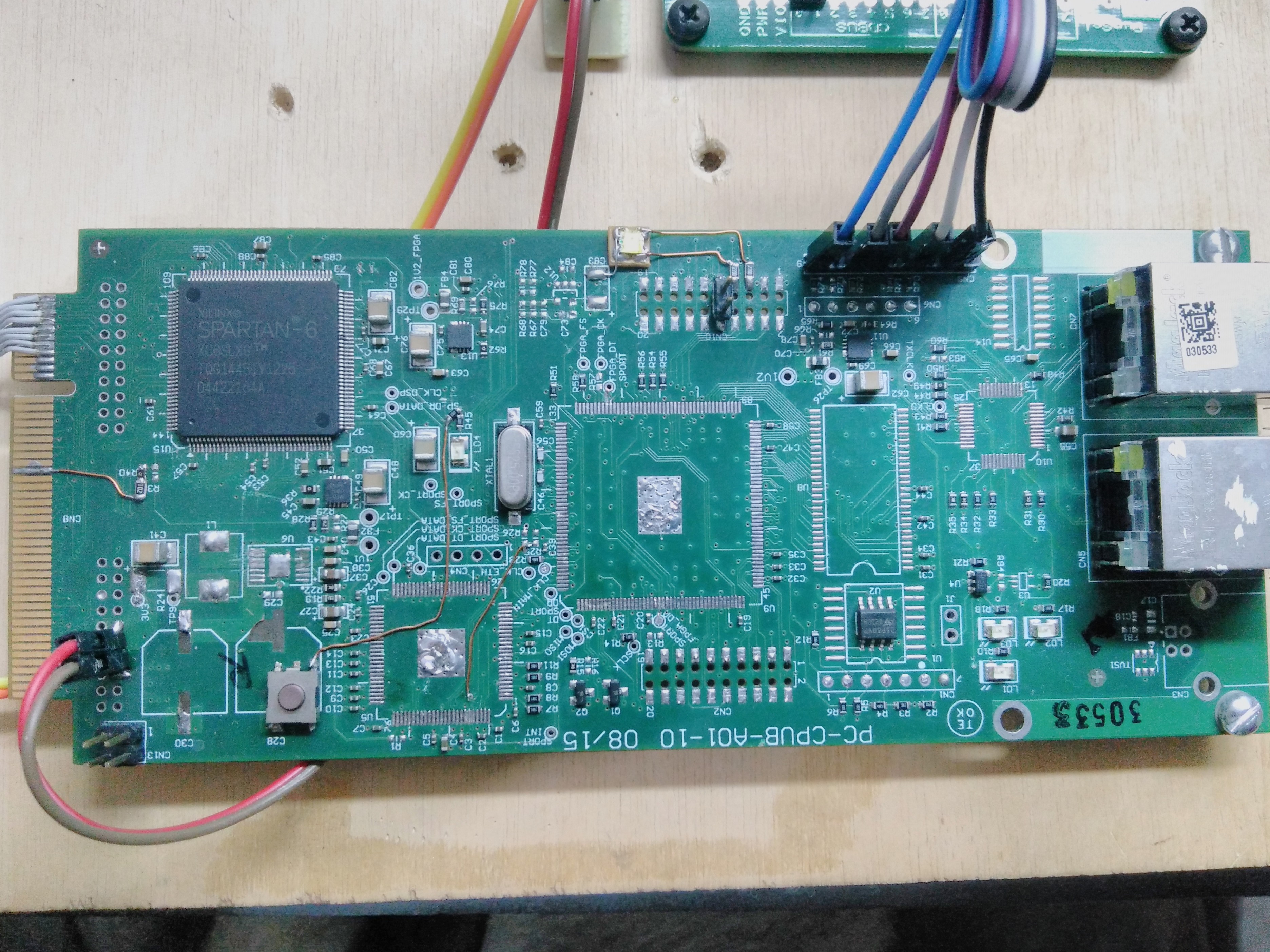
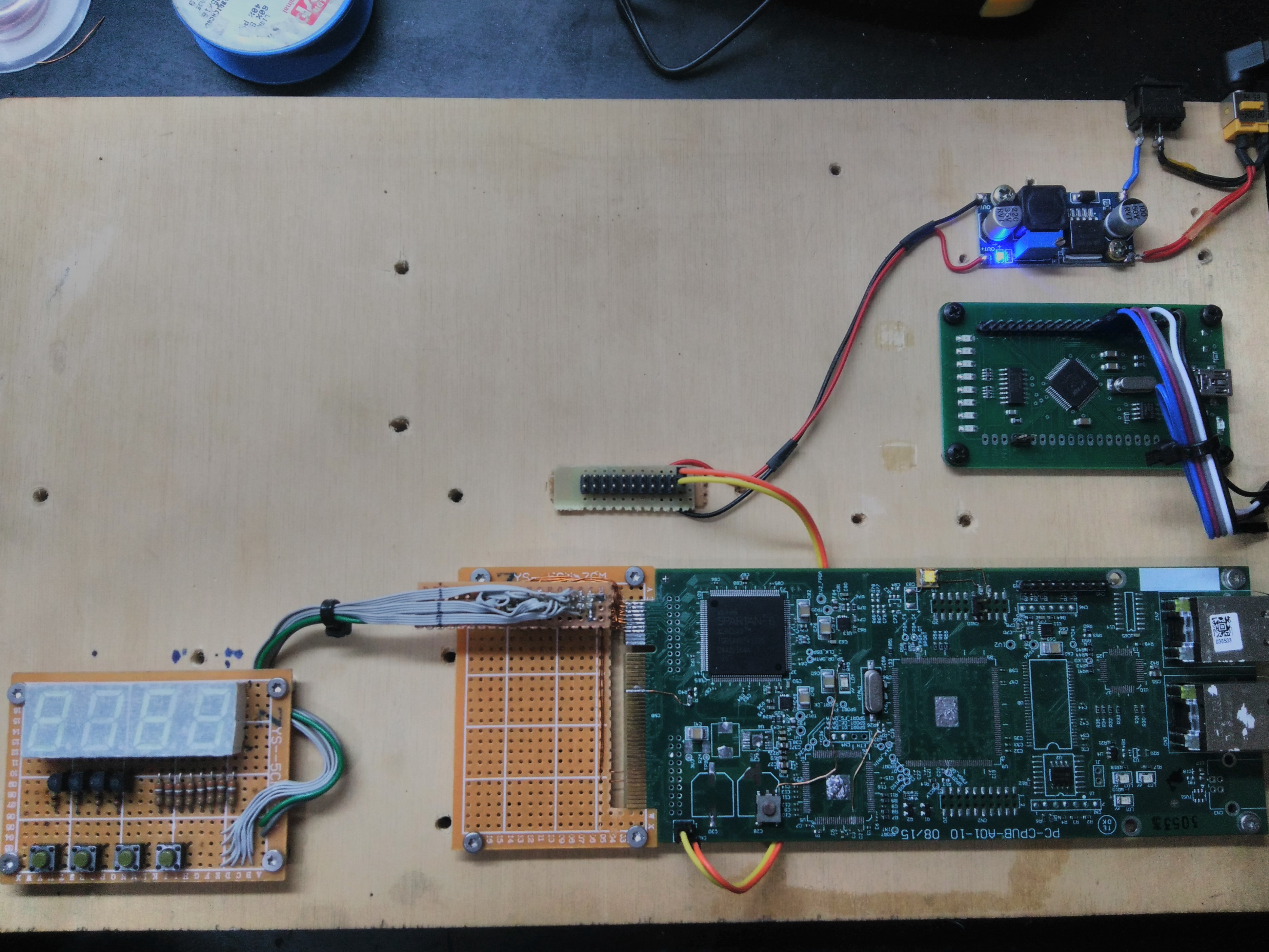
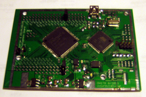
The board contains a Xilinx Spartan 6 FPGA (XC6SLX9TQG144), TI Sitara AM1705, SRAM, Ethernet PHY with 2 MagJacks and one ADSP from Analog Devices.
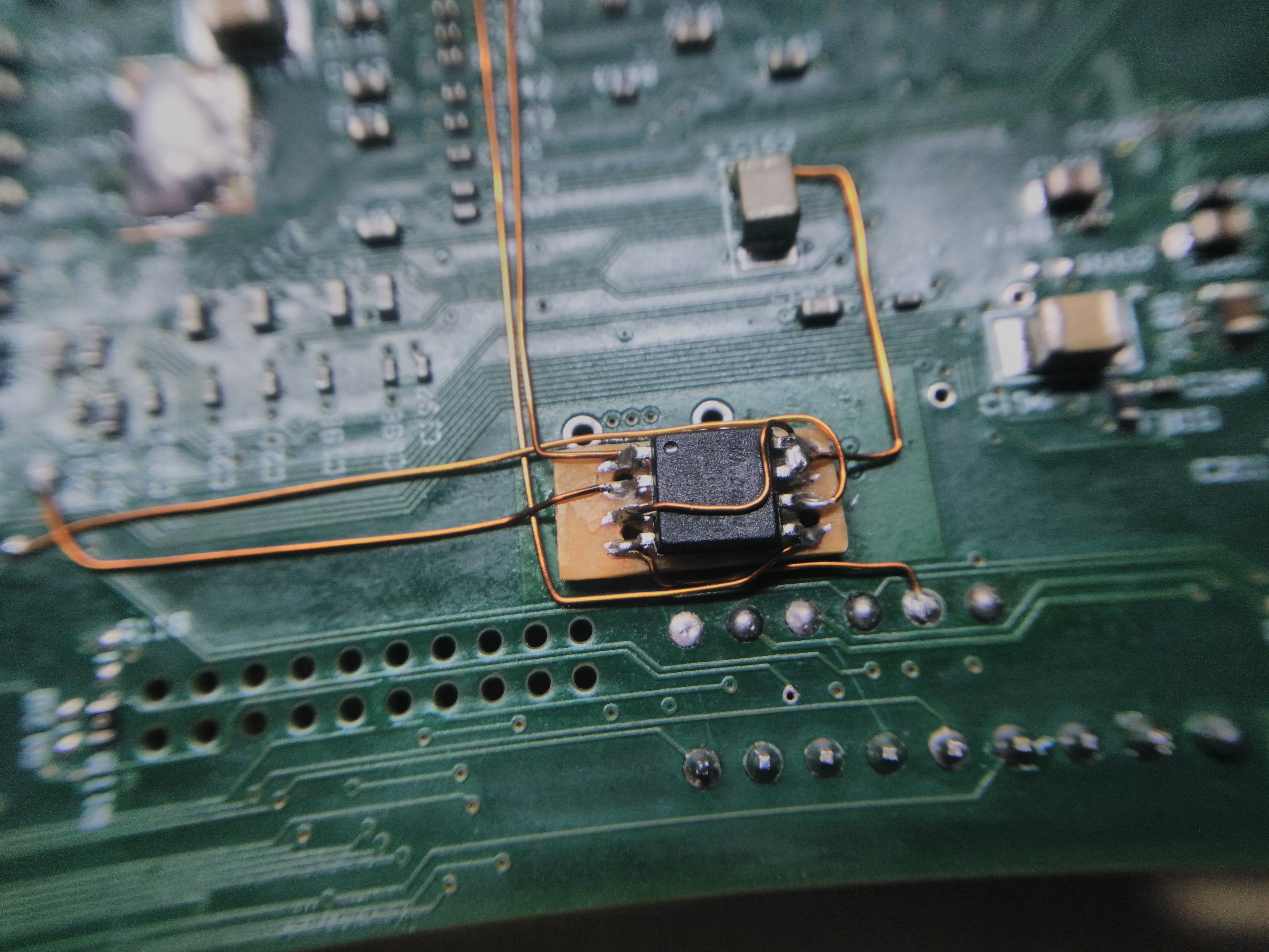
In one of my atempts to power up the board I destroyed the ADSP, RAM and the PHY :disappointed:.
But the good news was that the FPGA (and probably the Sitara, I haven't tested yet) was still working.
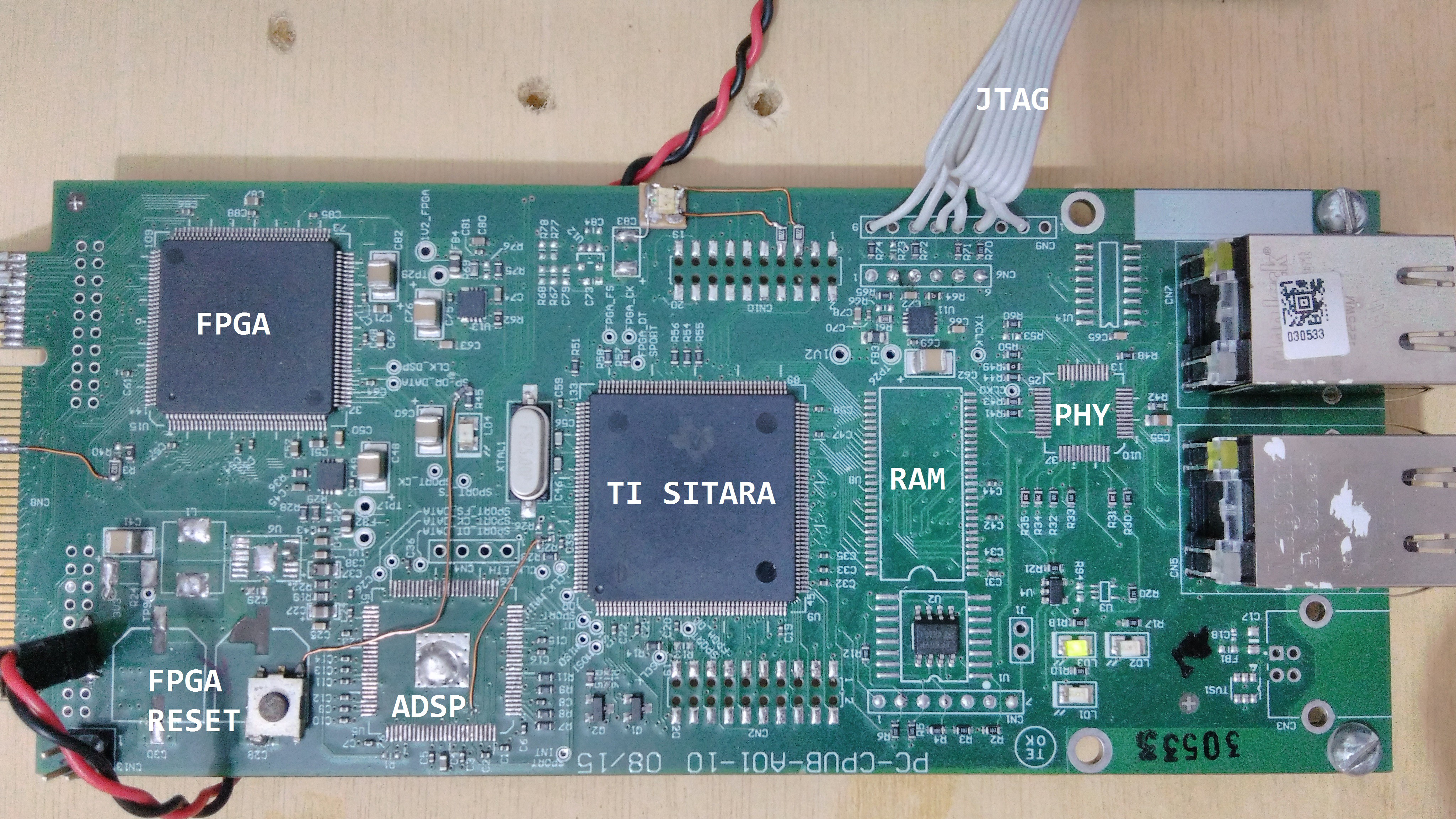
After some time triyng to find the JTAG traces in the board and using one FT2232 breakout board with OpenOCD was possible to execute JTAG commands and send the bitstream created with the Xilinx ISE to the FPGA.
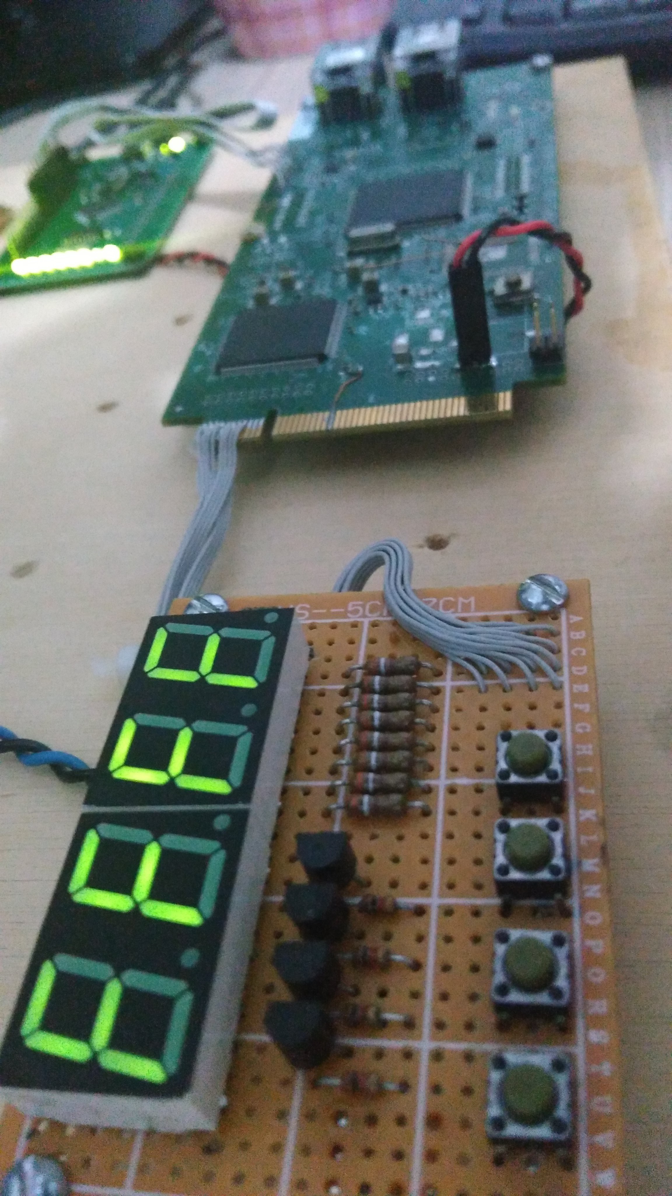
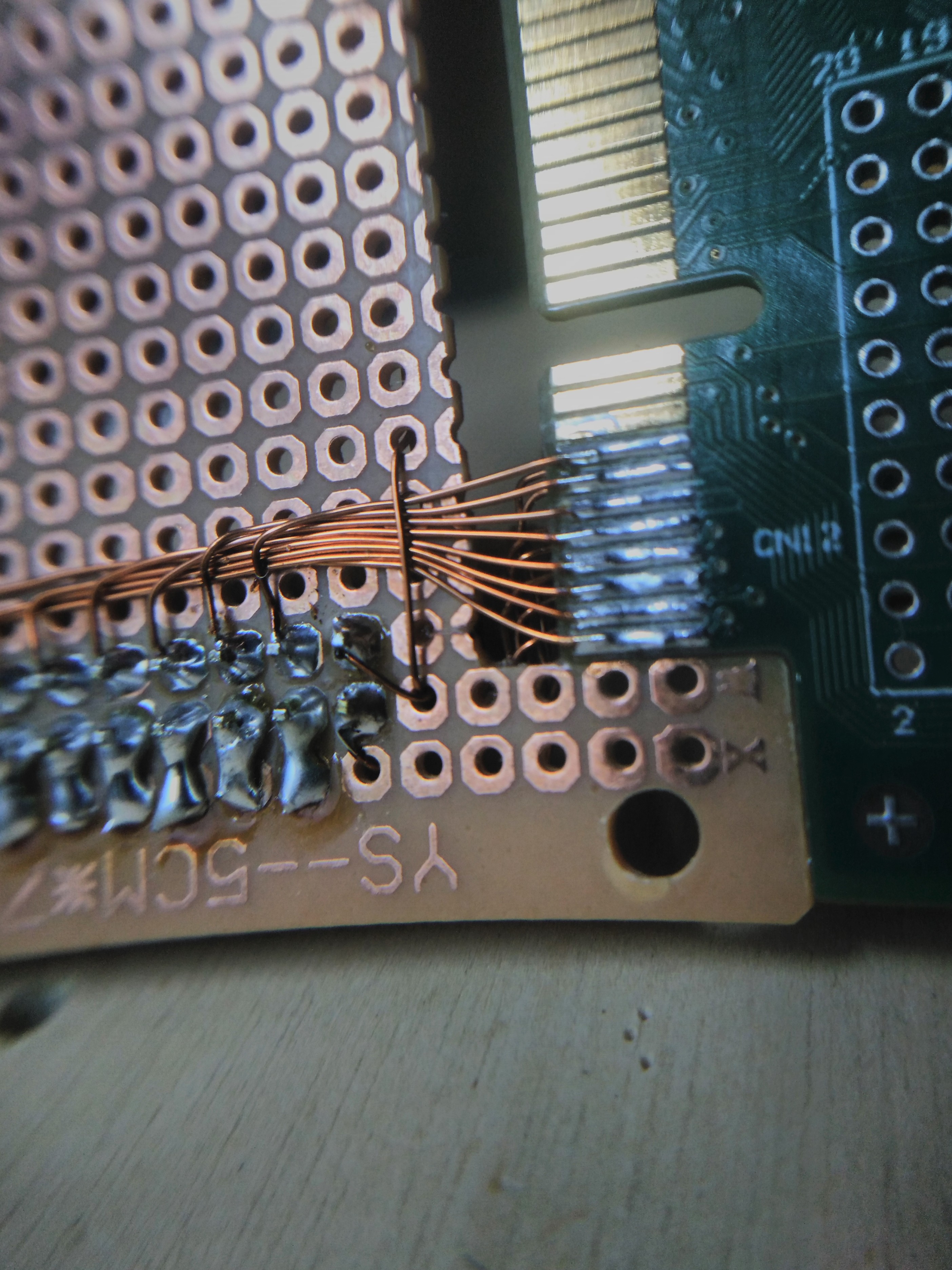
In this board, the FPGA was responsible for the communication between some other carrier board, a great amount of GPIOs are exposed on the edge connector. Using these GPIOs I've build a 4 digit 7 segment display board with 4 buttons.
 TommiRouvali
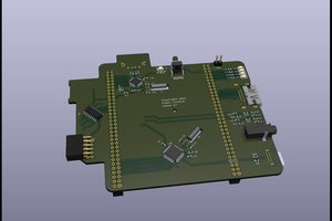
 ciborg971
 Dave's Dev Lab